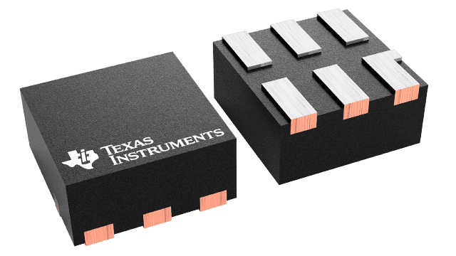
SN74LVC1G18DSFR
One of Two Noninverting Demultiplexer with 3-State Deselected Output
Description
Reviews
Features for the SN74LVC1G18
- Operating temperature from –40°C to +125°C
- Supports 5-V VCC operation
- Inputs accept voltages to 5.5 V
- Supports down translation to VCC
- Max tpd of 3.4 ns at 3.3 V
- Low power consumption, 10-µA max ICC
- ±24-mA Output drive at 3.3 V
- Typical VOLP (output ground bounce)
<0.8 V at VCC = 3.3 V, TA = 25°C - Typical VOHV (output VOH undershoot)
>2 V at VCC = 3.3 V, TA = 25°C - Ioff Supports live insertion, partial-power-down mode, and back-drive protection
- Latch-up performance exceeds 100 mA
Per JESD 78, Class II - ESD protection exceeds JESD 22
- 2000-V Human-body model (A114-A)
- 200-V machine model (A115-A)
- 1000-V Charged-device model (C101)
Description for the SN74LVC1G18
This non-inverting demultiplexer is designed for 1.65-V to 5.5-V VCC operation.
The SN74LVC1G18 device is a 1-of-2 non-inverting demultiplexer with a 3-state output. This device buffers the data on input A and passes it to either output Y0 or Y1, depending on whether the state of the select (S) input is low or high, respectively.
NanoFree™ package technology is a major breakthrough in IC packaging concepts, using the die as the package.
This device is fully specified for partial-power-down applications using Ioff. The Ioff circuitry disables the outputs, preventing damaging current backflow through the device when it is powered down.
Share your thoughts
Showing
6
of
0
reviews
Most recent
Top Reviews
Read more
Your rating
Your review *
Name *
Enter your Name
Email *
Enter your Email
Upload Image
Notice: Ensure your image is no larger than 200KB before uploading.
Submit
Contact Us Now
Enter your inquiry details, We will reply you in 24 hours.
Name can't be empty
E-mail can't be empty
Company can't be empty
Phone can't be empty
Phone
Products can't be empty
Products you want
Message can't be empty
Verification code error
Clear
People who viewed this item also viewed


